


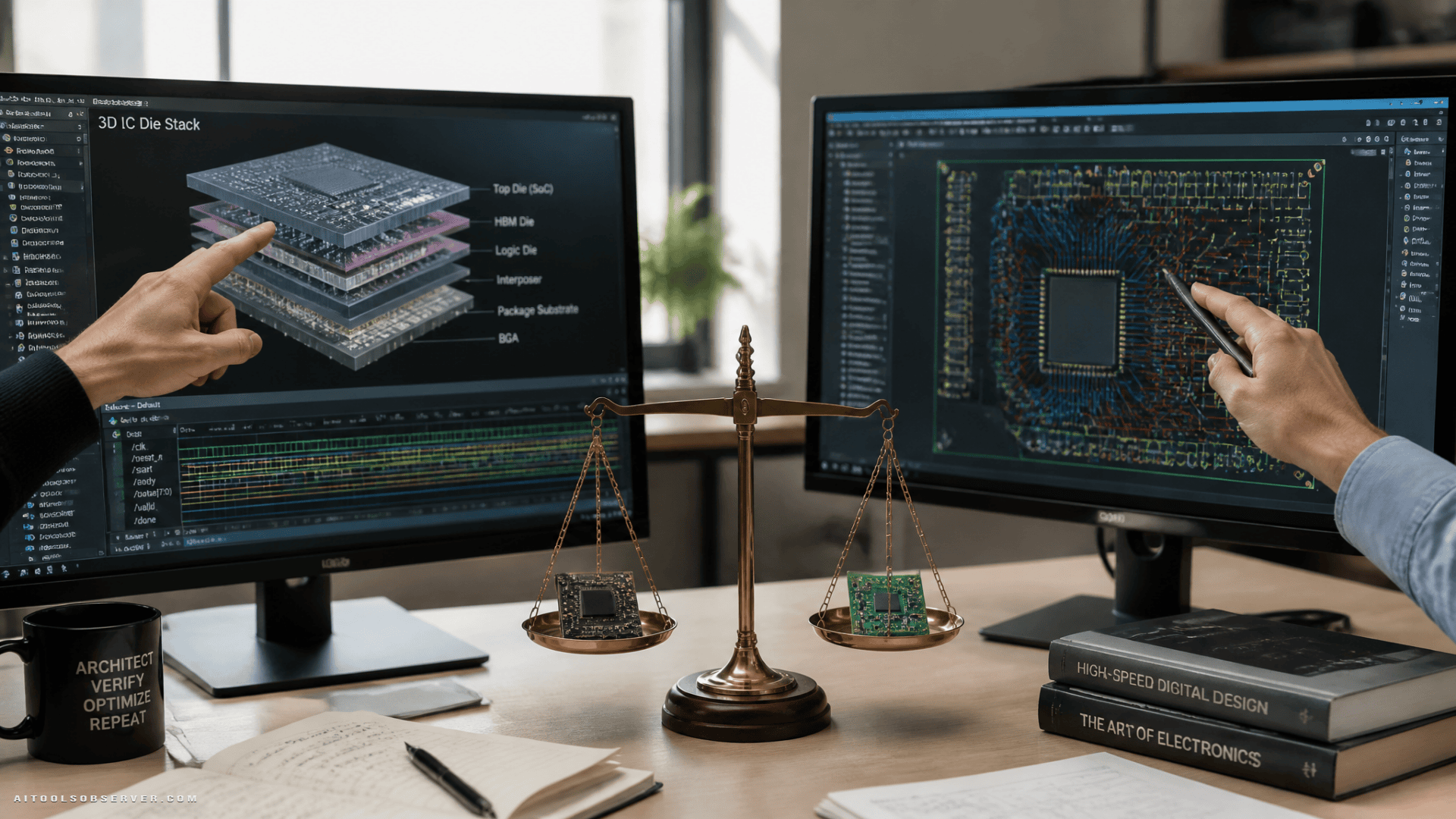
What Each Platform Is Trying to Solve
Both platforms address the same core problem: traditional EDA workflows are too slow for the complexity of modern designs. Where they differ is in scope, architecture, and the specific pain points they target first.
Siemens Fuse EDA AI Agents are positioned as a broad, portfolio-wide acceleration layer. Siemens has combined its existing EDA tools—including Catapult for synthesis, Questa One and Veloce for verification, Solido for custom IC design, Aprisa for physical implementation, Calibre for signoff, Tessent for design-for-test, Innovator3D IC for 3D integration, and Xpedition for PCB design—with Nvidia accelerated computing and CUDA-X libraries. The stated ambition is to speed up design tools by 1,000x, translating into overall productivity improvements of up to 50x.
Cadence AuraStack AI Super Agent is built on top of the existing Allegro AI Studio platform and is explicitly positioned as a full-flow agent spanning digital and analog silicon, advanced packaging, and PCB design. Cadence claims it is the only provider with agentic AI covering this entire design spectrum. AuraStack sits alongside other Cadence agents—ChipStack, InnoStack, and ViraStack—forming a broader agentic ecosystem.
Agentic AI: Autonomy, Trust, and Practical Adoption
Both platforms use the term agentic AI, but the practical implications deserve scrutiny.
Siemens frames agentic engineering as the orchestration of multi-domain verification at scale—agents that can reason across billions of test scenarios. This is primarily a verification and signoff story, aimed at the most computationally intensive parts of semiconductor design.
Cadence positions AuraStack as an agent that can take a concept to final product readiness, automating repetitive and iterative tasks across the full design flow. The ambition is broader, but Altavilla’s assessment is measured: broad adoption of fully agentic workflows will take time because engineers need to build trust before delegating more of the design process to the system.
This trust gap is the central adoption challenge for both platforms. Engineers will want to understand why the AI is making specific design decisions before they extend it more autonomy. Transparency mechanisms—explainability, audit trails, override controls—will likely determine how quickly either platform moves from task automation to genuine workflow orchestration.
Where Each Platform Has an Edge
Siemens Fuse EDA AI Agents appear better suited for teams working on leading-edge semiconductor design—particularly those dealing with 3D ICs, chiplets, and complex verification challenges. The depth of tool integration across synthesis, simulation, physical implementation, and signoff makes it a coherent choice for organizations already invested in the Siemens EDA ecosystem.
Cadence AuraStack appears more immediately accessible and more explicitly designed for PCB and packaging workflows. The cross-discipline integration story—breaking down silos between electrical, mechanical, thermal, and packaging teams—addresses a real organizational friction point. The accessibility positioning, including support for small companies, gives it a broader potential user base.
What to Watch Before Committing
Neither platform has disclosed pricing. Cadence has confirmed AuraStack is available now on Allegro AI Studio; Siemens has indicated its expanded AI-native EDA portfolio will arrive in forthcoming releases. This timing difference matters for teams evaluating near-term deployment.
The reported productivity figures—50x from Siemens, 100x substrate routing improvement from TSMC with Cadence—are compelling but come primarily from vendor statements and early customer testimonials. Independent, production-scale validation across diverse design environments has not yet been widely published.
The more useful question for engineering teams is not which platform claims the larger speedup, but which one integrates cleanly into the existing toolchain, supports the specific design domains in play, and provides enough transparency for engineers to build justified confidence in the AI’s decisions.
For semiconductor-focused teams with complex verification requirements, Siemens’ portfolio depth is the stronger argument. For PCB and packaging teams—especially those working across disciplines or at smaller scale—Cadence AuraStack’s accessibility and cross-domain integration make it the more immediately practical option.






Comments (0) No comments yet
Want to join this discussion? Login or Register.
No comments yet. Be the first to share your thoughts!